
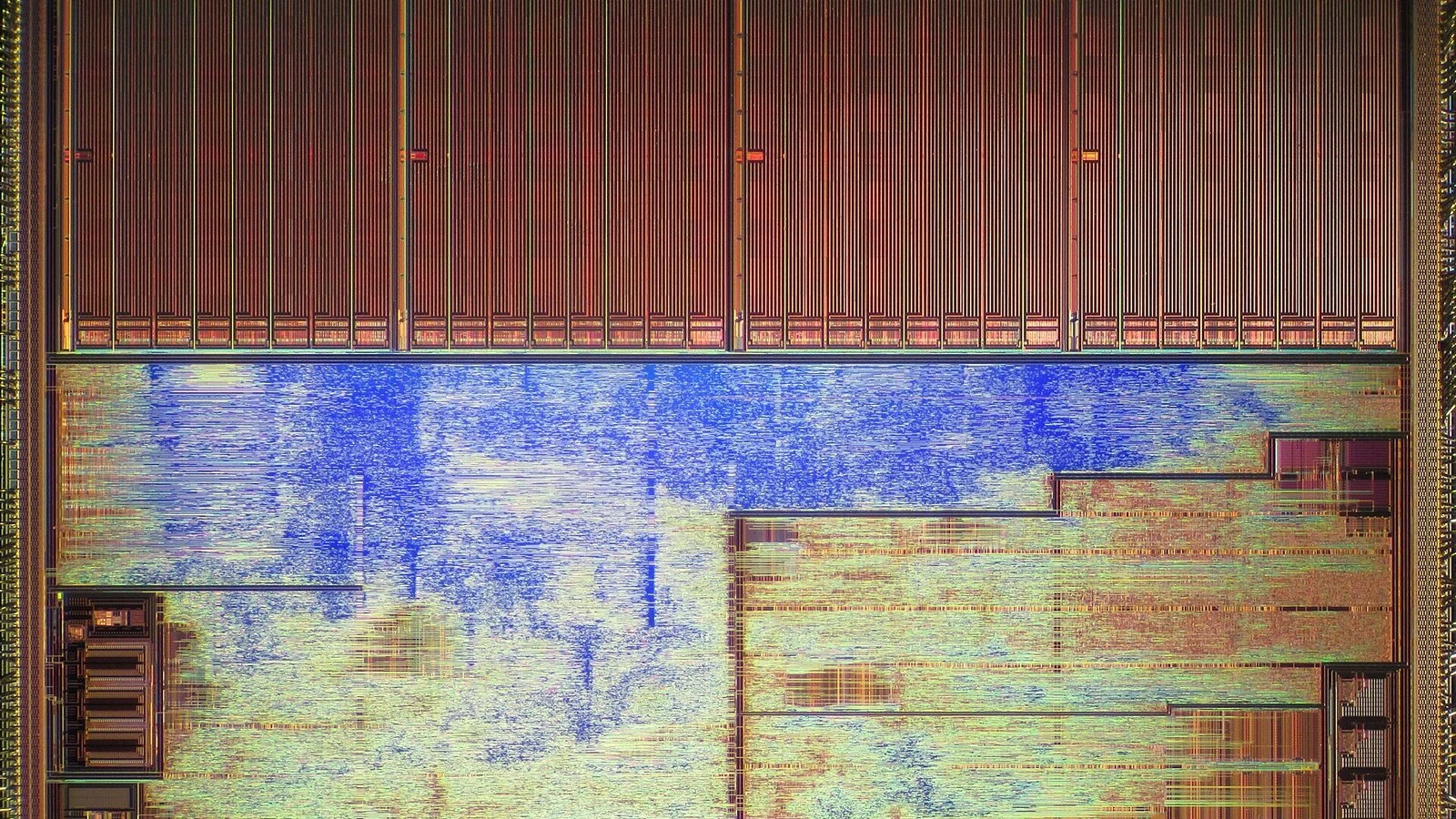
SemiAnalysis has torn down Intel’s Panther Lake, shipping as the Core Ultra 7 365, for the first detailed look at the Intel 18A node inside a chip that’s actually on sale. Its finding: 18A’s compute logic measures out at roughly the same density as TSMC’s N3E, the node used for Panther Lake’s own 12-core Xe3 GPU tile, but 18A does not overtake TSMC’s newer N3P and N2 nodes, or Samsung’s SF2, on peak density.
Inside the Intel 18A node: RibbonFET and PowerVia
Panther Lake is Intel’s first chip built with RibbonFET, the company’s gate-all-around transistor design: the gate wraps around the channel on all four sides instead of just three, which gives it tighter control over current leakage as transistors shrink. It’s paired with PowerVia, the first commercial implementation of backside power delivery, which moves the power wiring to the underside of the wafer and frees the front side entirely for signal routing. SemiAnalysis counted four stacked ribbons per transistor on 18A, one more than the three sheets it found on Samsung’s SF2.
The two technologies target different problems. Backside power delivery matters because moving power rails to the underside of the die cuts resistive losses in the wiring that carries current to each transistor, which is the main thing that limits how tightly a chip can be clocked before it runs hot. Freeing the front side for signal routing also gives designers more room to route logic without the two layers competing for space. TSMC is taking a similar path with its own N2 node, which pairs nanosheet transistors with a backside power option of its own, so Panther Lake isn’t testing an idea unique to Intel; it’s testing whether Intel can execute one at the same time as TSMC.
Using a representative-cell model, the firm puts 18A’s compute logic at roughly 18.6% denser than the Intel 3 GPU logic it replaces. TechPowerUp’s write-up carries the rest of the die-level figures: the Cougar Cove P-core occupies about the same area as Lunar Lake’s Lion Cove despite its L2 cache growing from 2.5MiB to 3MiB, and the NPU 5 block needs 36.9% less die area than Lunar Lake’s NPU 4 while keeping the same number of INT8 MAC units. SemiAnalysis describes the CPU cores themselves as incremental updates rather than a clean-sheet design.
Where TSMC still leads on density
None of that hands Intel a manufacturing lead. SemiAnalysis is explicit that 18A does not lead TSMC’s N3P or N2, or Samsung’s SF2, in peak density, and it cautions that a single representative-cell figure doesn’t settle which foundry wins across an entire die: whole-chip density depends heavily on cell mix and how densely each block is actually placed. For Panther Lake’s owners this changes nothing about the laptop they already bought. What it does affect is whether Intel Foundry can win outside customers away from TSMC on the strength of the process alone.
What this means for Intel’s 14A promise
We reported two days ago that Intel expects its next node, 14A, to land within 5% of TSMC’s A14, a figure that came from Intel itself rather than from independent measurement. This teardown is the closest thing to an independent check available before 14A ships, and it’s not flattering: 18A ties TSMC’s N3E but sits behind N3P, N2 and SF2. If 14A is meant to close the gap with TSMC’s next generation, it’s starting from a node that’s already behind on the generation TSMC ships today. Whether Intel closes that gap or merely narrates it will need the same kind of teardown, not another vendor slide.
Image: Pauli Rautakorpi via Wikimedia Commons, licensed under CC BY 3.0.